Product Summary
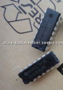
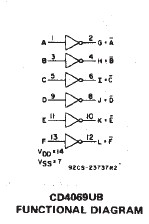
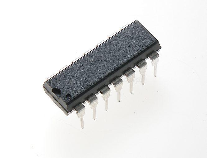
The CD4069UBE consists of six CMOS inverter circuits and this device is supplied in 14-lead hermetic dual-in-line ceramic pack- ages (D and Fsuffixes), 14-leaddual-in-line plastic package (E suffix), and in chip form (H suffix). The CD4069UBE is intended for all general-purpose inverter applications where the medium-power TTL- drive and logic-level-conversion capabilities of circuits such as the CD4009 and CD4049 Hex Inverter/Buffers are not required.
Parametrics
CD4069UBE absolute maximum ratings:(1)DC supply-voltage range, (VDD) voltages referenced to VSS terminal): -0.5V to +20V; (2)input voltage range, all inputs: -0.5V to VDD + 0.5V; (3)DC input current, any one input: 士10mA; (4)power dissipation per package (PD): For TA = -55℃ to +100℃: 500m W; for TA+100℃ to +125℃: derate linearly at 12W/℃ to 200mW; (5)device dissipation per output transistor for TA=full package-temperature range (all package tyres): 100mW; (6)operating-temperature range (TA): -55℃ to 125℃; (7)storage temperature range (Tstg): -65℃ to +150℃.
Features
CD4069UBE features: (1)standardized symmetrical output characteristics; (2)medium Speed at 70V; (3)operation-tpHL, tpLH=30 ns (typ) at 10V; (4)100% tested for quiescent current at 20 V; (5)maximum input current of 1 μA at 18 V over full package-temperature range; 100 nA at 18 V and 25℃; (6)meets all requirements of JEDEC tentative standard No. 138, "standard specifications for description of B Series.CMOS Devices".
Diagrams
| Image | Part No | Mfg | Description |  |
Pricing (USD) |
Quantity | ||||||||||||
|---|---|---|---|---|---|---|---|---|---|---|---|---|---|---|---|---|---|---|
 |
 CD4069UBE |
 Texas Instruments |
 Inverters Hex |
 Data Sheet |

|
|
||||||||||||
 |
 CD4069UBEE4 |
 Texas Instruments |
 Inverters CMOS HEX INVERTER |
 Data Sheet |

|
|
||||||||||||
 (China (Mainland))

