(China (Mainland))

Product Summary
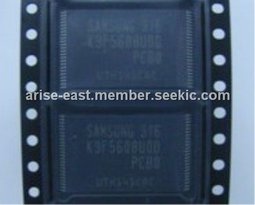
The K9F5608UOD-PCBO is a 256M bit with spare 8M bit capacity. The K9F5608UOD-PCBO is offered in 1.8V, 2.65V, 3.3V Vcc. Its NAND cell provides the most cost-effective solutIon for the solid state mass storage market. A program operation can be performed in typical 200ms on a 528-byte(X8 device) or 264-word(X16 device) page and an erase operation can be performed in typical 2ms on a 16K-byte(X8 device) or 8K-word(X16 device) block. Data in the page can be read out at 50ns cycle time per word. The I/O pins serve as the ports for address and data input/output as well as command input. The on-chip write control automates all program and erase functions including pulse repetition, where required, and internal verification and margining of data. Even the write-intensive systems can take advantage of the K9F5608UOD-PCBO extended reliability of 100K program/erase cycles by providing ECC(Error Correcting Code) with real time mapping-out algorithm. The K9F5608UOD-PCBO is an optimum solution for large nonvolatile storage applications such as solid state file storage and other portable applications requiring non-volatility.
Parametrics
K9F5608UOD-PCBO absolute maximum ratings: (1)Voltage on any pin relative to VSS VIN/OUT: -0.6 to + 2.45, -0.6 to + 4.6v; (2)Voltage on any pin relative to VSS VIN/OUT: -0.2 to + 2.45 -0.6 to + 4.6v; (3)Voltage on any pin relative to VSS VIN/OUT: -0.2 to + 2.45 -0.6 to + 4.6v; (4)Temperature Under Bias K9F56XXX0C-XCB0 TBIAS: -10 to +125°C; (5)Temperature Under Bias K9F56XXX0C-XIB0 TBIAS: -40 to +125°C; (6)Storage Temperature K9F56XXX0C-XCB0 TSTG: -65 to +150°C; (7)Short Circuit Current Ios: 5 mA.
Features
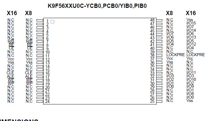
K9F5608UOD-PCBO features: (1)Command/Address/Data Multiplexed I/O Port; (2)Hardware Data Protection: Program/Erase Lockout During Power Transitions; (3)Reliable CMOS Floating-Gate Technology: Endurance : 100K Program/Erase Cycles, Data Retention : 10 Years; (4)Command Register Operation; (5)Intelligent Copy-Back; (6)Unique ID for Copyright Protection; (7)Power-On Auto-Read Operation; (8)Safe Lock Mechanism.(http://www.alldatasheet.com/datasheet-pdf/pdf/136613/SAMSUNG/K9F5608UOC.html)
Diagrams
 |
 K9F5608D0C |
Other |
|
Data Sheet |
Negotiable |
|
||||
|
K9F5608D0D |
Other |
|
Data Sheet |
Negotiable |
|
||||
|
K9F5608Q0B-DCB0 |
Other |
|
Data Sheet |
Negotiable |
|
||||
|
K9F5608Q0B-DIB0 |
Other |
|
Data Sheet |
Negotiable |
|
||||
|
K9F5608Q0B-HCB0 |
Other |
|
Data Sheet |
Negotiable |
|
||||
|
K9F5608Q0B-HIB0 |
Other |
|
Data Sheet |
Negotiable |
|
||||