(China (Mainland))


Product Summary
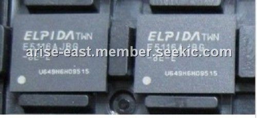
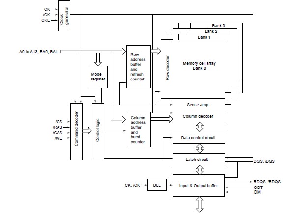
The EDE5116AJBG-8E-E is a 512M bits DDR2 SDRAM.
Parametrics
EDE5116AJBG-8E-E absolute maximum ratings: (1)Power supply voltage VDD: -1.0 to +2.3 V; (2)Power supply voltage for output VDDQ:-0.5 to +2.3 V ; (3)Input voltage VIN: -0.5 to +2.3 V ; (4)Output voltage VOUT: -0.5 to +2.3 V ; (5)Storage temperature Tstg: -55 to +100 °C ; (6)Power dissipation PD: 1.0 W ; (7)Short circuit output current IOUT: 50 mA.
Features
EDE5116AJBG-8E-E features: (1)Double-data-rate architecture; two data transfers per clock cycle; (2)The high-speed data transfer is realized by the 4 bits prefetch pipelined architecture; (3)Bi-directional differential data strobe (DQS and /DQS) is transmitted/received with data for capturing data at the receiver; (4)DQS is edge-aligned with data for READs; centeraligned with data for WRITEs; (5)Differential clock inputs (CK and /CK); (6)DLL aligns DQ and DQS transitions with CK transitions; (7)Commands entered on each positive CK edge; dataand data mask referenced to both edges of DQS; (8)Data mask (DM) for write data; (9)Posted /CAS by programmable additive latency for better command and data bus efficiency; (10)Off-Chip-Driver Impedance Adjustment and On-Die- Termination for better signal quality; (11)Programmable RDQS, /RDQS output for making× 8 organization compatible to× 4 organization; (12)/DQS, (/RDQS) can be disabled for single-ended Data Strobe operation.
Diagrams
 |
 EDE5104ABSE |
Other |
|
Data Sheet |
Negotiable |
|
||||
|
EDE5104AESK |
Other |
|
Data Sheet |
Negotiable |
|
||||
|
EDE5104AGSE |
Other |
|
Data Sheet |
Negotiable |
|
||||
|
EDE5104AGSE-5C-E |
Other |
|
Data Sheet |
Negotiable |
|
||||
|
EDE5104GBSA |
Other |
|
Data Sheet |
Negotiable |
|
||||
|
EDE5108ABSE |
Other |
|
Data Sheet |
Negotiable |
|
||||